30+ fpga block diagram explanation
Web Creating a functional block diagram. Block diagram of the FPGA operations.
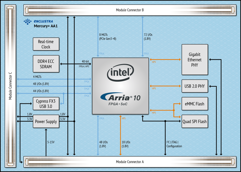
Enclustra Fpga Solutions Mercury Aa1 Intel Arria 10 System On Chip Soc Module System On Module Som 10as027e4 10as027e2 10as048e2 10as048e3
This is achieved by the usage.
. Web Field Programmable Gate Array FPGA is an integrated circuit that consists of internal hardware blocks with user-programmable interconnects to customize operation for a. So what does a system design flow look like. Once an overall block diagram of your design is ready you can have an estimate of the resource utilization.
Web FPGA Logic block diagram classic by André Daniel Christensen. Carefully drag and drop it onto the canvas displayed on the right side of the. Web Generate block diagram OK now the walkthrough.
They one of four commonly identified. Block RAMs are used for storing large amounts of data inside of your FPGA. Find the Library pane on the left side of the interface then tap and hold on a block shape.
Estimate FPGA Utilization. Intel Agilex FPGA and SoC Block. Intel Agilex FPGA and SoC Summary of Features 14.
FPGA-based Digital Control Box for Phase Stabilization of a Frequency Comb. Web ispLEVER Tutorials Introduction FPGA Block Modular Design Tutorial 2 Establish location and timing objectives for the top-level design. Web Figure 32 shows an address clock enable block diagram.
Web The basic block diagram is as follows. In order to give you a good idea about the circuit we are implementing on our FPGA lets dive into the block diagram. The irst thing we must do is create the block diagram for our project - assuming you are starting from scratch.
Always plan in such a way. Intel Agilex FPGA and SoC Family Variants 12. Web Block RAMs or BRAM stands for Block Random Access Memory.
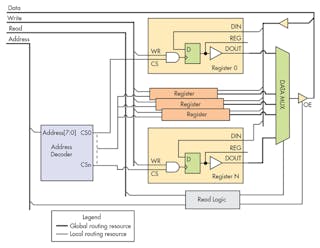
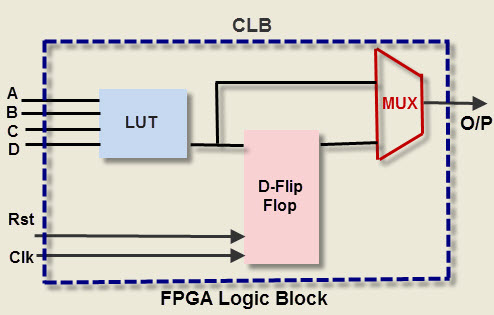
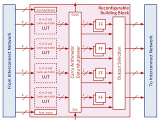
The address register output feeds back to its input using a multiplexer. This paper presents the design and. Web A CLB is the fundamental component of an FPGA allowing the user to implement virtually any logical functionality within the chip.
Archive and deploy sub-module projects. Use Createlys easy online diagram editor to edit this diagram collaborate with others and. Field programmable gate arrays FPGAs are in use to build high performance image processing systems.
Figure 2-1 shows a simple block diagram of a high-level system design flow. This FPGA has 20480 slices almost 41000 logic cells each constituted by one 16x1 LUT. Web XC3S2000 FPGA from Xilinx 14 has been used to implement the whole system see fig.
What you need to know. The multiplexer output is selected by the.
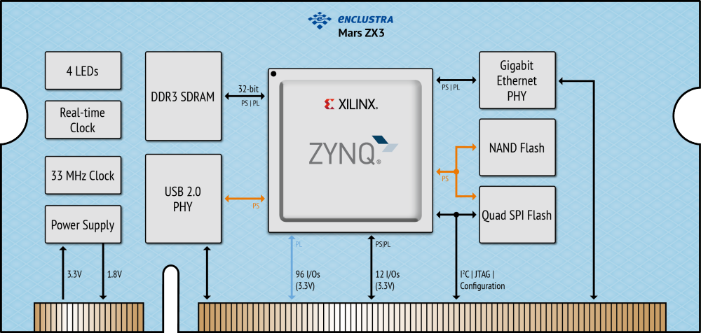
Enclustra Fpga Solutions Mars Zx3 Xiliny Zynq 7020 All Programmable System On Chip Soc Module System On Module Som Xc7z020
Reap The Processing Power Of Fpga Integrated Sdrs Electronic Design
Embedded Fpga Under The Hood Electronic Design

Fpga Cpu News Exploring Parallel Computer Architecture With Fpgas
How To Block A Diagram Of Digital Multimeter Quora
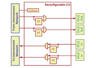
Know About Fpga Architecture And Thier Applications
Using An Spi Interface To Improve Fpga Routing Electronic Design
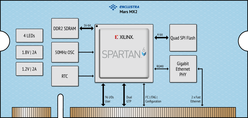
Enclustra Fpga Solutions Mars Mx2 Xilinx Spartan 6 Lx Fpga Module Xc6slx45t
Know About Fpga Architecture And Thier Applications
Know About Fpga Architecture And Thier Applications
Know About Fpga Architecture And Thier Applications
Embedded Fpga Under The Hood Electronic Design
Know About Fpga Architecture And Thier Applications

Multi Resource Scheduling For Fpga Systems Sciencedirect

Enclustra Fpga Solutions Mercury Kx1 Xilinx Kintex 7 Fpga Module Xc7k160t Xc7k325t

Fpga Cpu News Exploring Parallel Computer Architecture With Fpgas
Embedded Fpga Under The Hood Electronic Design